


Published on Apr 02, 2024
Nano electronic devices fall into two classes: tunnel devices and ballistic transport devices. In Tunnel devices single electron effects occur if the tunnel resistance is larger than h/e = 25 K §Ù. In Ballistic devices with cross sectional dimensions in the range of quantum mechanical wavelength of electrons, the resistance is of order h/e = 25 K §Ù.
This high resistance may seem to restrict the operational speed of nano electronics in general. However the capacitance values and drain source spacing are typically small which gives rise to very small RC times and transit times of order of ps or less.
Thus the speed may be very large, up to THz range. The goal of this seminar is to present the models an performance predictions about the effects that set the speed limit in carbon nanotube transistors, which form the ideal test bed for understanding the high frequency properties of Nano electronics because they may behave as ideal ballistic 1d transistors.
When carriers travel through a semiconductor material, they are likely to be scattered by any number of possible sources, including acoustic and optical phonons, ionized impurities, defects, interfaces, and other carriers. If, however, the distance traveled by the carrier is smaller than the mean free path, it is likely not to encounter any scattering events; it can, as a result, move ballistically through the channel. To the first order, the existence of ballistic transport in a MOSFET depends on the value of the characteristic scattering length (i.e. mean free path) in relation to channel length of the transistor.
This scattering length, l , can be estimated from the measured carrier mobility where t is the average scattering time, m* is the carrier effective mass, and vth is the thermal velocity. Because scattering mechanisms determine the extent of ballistic transport, it is important to understand how these depend upon operating conditions such as normal electric field and ambient temperature.
In state-of-the-art MOSFET inversion layers, carrier scattering is dominated by phonons, impurities (Coulomb interaction), and surface roughness scattering at the Si-SiO2 interface. The relative importance of each scattering mechanism is dependent on the effective electric field component normal to the conduction channel. At low fields, impurity scattering dominates due to strong Coulombic interactions between the carriers and the impurity centers. As the electric field is increased, acoustic phonons begin to dominate the scattering process. At very high fields, carriers are pulled closer to the Si-SiO2 gate oxide interface; thus, surface roughness scattering degrades carrier mobility. A universal mobility model has been developed to relate field strength with the effective carrier mobility due to phonon and surface roughness scattering:
When the temperature is changed, the relative importance of each of the aforementioned scattering mechanisms is altered. Phonon scattering becomes less important at very low temperatures. Impurity scattering, on the other hand, becomes more significant because carriers are moving slower (thermal velocity is decreased) and thus have more time to interact with impurity centers. Surface roughness scattering remains the same because it does not depend on temperature. At liquid nitrogen temperatures (77K) and an effective electric field of 1MV/cm, the electron and hole mobilities are ~700 cm2/Vsec and ~100 cm2/Vsec, respectively. Using the above equations, the scattering lengths are approximately 17nm and 3.6nm.These scattering lengths can be assumed to be worst-case scenarios, as large operating voltages (1V) and aggressively scaled gate oxides (10Å) are assumed. Thus, actual scattering lengths will likely be larger than the calculated values.
Further device design considerations in maximizing this scattering length will be discussed in the last section of this paper. Still, the values calculated above are certainly in the range of transistor gate lengths currently being studied in advanced MOSFET research (<50nm). Ballistic carrier transport should thus become increasingly important as transistor channel lengths are further reduced in size. In addition, it should be noted that the mean free path of holes is generally smaller than that of electrons. Thus, it should be expected that ballistic transport in PMOS transistors is more difficult to achieve, since current conduction occurs through hole transport. Calculation of the mean scattering length, however, can only be regarded as a first-order estimation of ballistic transport.
To accurately determine the extent of ballistic transport evident in a particular transistor structure, Monte Carlo simulation methods must be employed. Only by modeling the random trajectory of each carrier traveling through the channel can we truly assess the extent of ballistic transport in a MOSFET.
In state-of-the-art MOSFET inversion layers, carrier scattering is dominated by phonons, impurities (Coulomb interaction), and surface roughness scattering at the Si-SiO2 interface. As shown in Figure 2, the relative importance of each scattering mechanism is dependent on the effective electric field component normal to the conduction channel. At low fields, impurity scattering dominates due to strong Coulombic interactions between the carriers and the impurity centers. As the electric field is increased, acoustic phonons begin to dominate the scattering process. At very high fields, carriers are pulled closer to the Si-SiO2 gate oxide interface; thus, surface roughness scattering degrades carrier mobility. A universal mobility model has been developed to relate field strength with the effective carrier mobility due to phonon and surface roughness scattering:
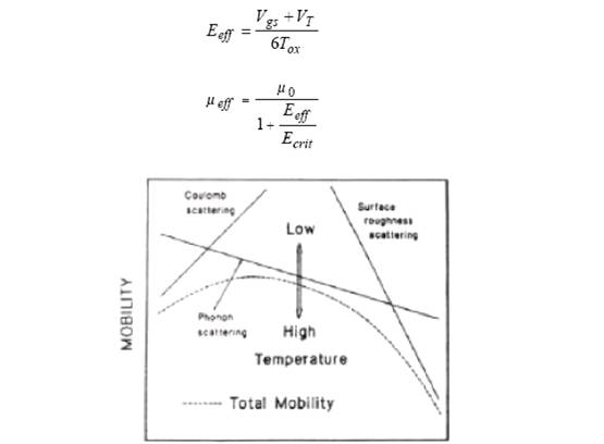
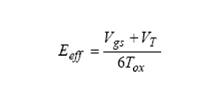
where Vgs is the applied gate voltage, VT is the transistor threshold voltage, Tox is the gate oxide thickness, and mO and Ecrit are empirically-derived constants. As predicted by the International Technology Roadmap for Semiconductors ,device technologies at near ballistic (~30nm) channel lengths will have power supplies of <0.8V, VT<0.2V, Tox,eq~10A. This yields an effective electric field of approximately ~lMV/cm. The actual value may be lower, depending on the actual device structure and operating conditions. With doping concentrations in the channel region of the MOSFET expected to be on the order of 1018, from ,we find that the electron mobility is -230 cm2/Vsec and the hole mobility is -65 cm2/Vsec at room temperature. This yields scattering lengths of approximately 5.5nm and 2.4nm.
As evidenced by preceding sections, ballistic transport allows for larger transistor saturation currents because carriers are experience no scattering. Designing future transistors to maximize the likelihood of ballistic transport is thus highly desirable. As shown ,simply by shrinking current transistor designs, a significant step can be taken towards this goal. However, modifications to the operating conditions or to the device structure itself may help to further induce ballistic transport. Recently, much interest has been placed on thin body double-gate MOSFET designs (Figure 4) due to its superior immunity to detrimental short-channel effects.
This structure, in particular, lends itself to the promotion of ballistic carrier transport due to its low-doped channel and dual-gate nature. The following briefly describes some techniques that may be used in the design of future transistor technologies to minimize carrier scattering, thus promoting ballistic transport. The primary goal is to reduce the likelihood of scattering events in the MOSFET inversion layer and increase the mean free path. Minimizing surface roughness scattering Because of the large electric fields experienced by carriers in MOSFET inversion layers, scattering is due predominately to interface roughness.
To minimize the impact of this scattering mechanism, the problem can be attacked from two perspectives: improving the Si-SiO2 interface quality, and decreasing the normal electric field. The former will indeed reduce surface roughness scattering, but there is little room for improvement as current semiconductor process technologies are quite mature and yield very clean and smooth interfaces. Even so, it may be helpful to take precautions during processing to ensure a good interface; this may include ion implantation through a screen oxide, sacrificial oxidation steps to clean up surfaces after reactive ion etching, or dry as opposed to wet oxidation techniques. Decreasing the normal electric field is a more viable option. As mentioned earlier, the normal electric field can be expressed as:
To decrease the normal electric field, either the power supply voltage (which becomes the applied Vgs) must be scaled down or the oxide thickness must be increased. Lowering of the power supply is already a widespread trend, mainly due to power dissipation and device reliability concerns. However, this results in a smaller inversion charge density and thus a smaller current. As such, a tradeoff in current drive can be observed between minimization of carrier scattering and the decrease in inversion charge.
There is likely an optimum point for the choice of supply voltage. Normally, gate oxide thickness is decreased in advanced transistor technologies to combat short channel effects and to improve the ability to "turn off' the transistor. However, a thicker gate oxide may allow for ballistic transport, which may decrease the effective field, increase current, and result in an overall advantage. The double-gate MOSFET structure (Figure 4) is particularly attractive for this option because two gate electrodes exist to help to control channel conductivity, the gate oxide thickness need not be as thin to achieve small gate lengths.
| Are you interested in this topic.Then mail to us immediately to get the full report.
email :- contactv2@gmail.com |
